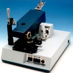
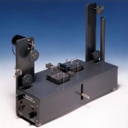
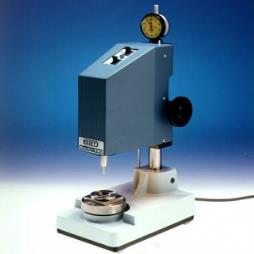
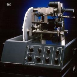
Backside Emission Analysis Preparation System (BEAPS)
Model 575 Advances in semiconductor technology have led to the introduction of multiple metal layers and even complete metal ground planes interconnected with vias. In today's advanced semiconductor designs, four or more layers of metallization can trap weak photon emissions beneath overlying metallization or force emissions at such low incident angles respective to the optics that even extended numerical aperture lenses are unable to detect them using front-side inspection techniques. The Model 575 Backside Emission Analysis Preparation System (BEAPS™) is a precision polishing station which provides a means to flat polish a large predefined area maintaining die planarity within 10 m with minimal user supervision. The BEAPS™ system utilizes a versatile stage which can either rotate or oscillate in both the X and Y directions and allows for a wide range of package and die sizes to be accommodated. Adjustments set by the user allow only selected areas of the package to be thinned, which helps prevent lead damage and other adverse effects traditionally encountered with standard back thinning methods. A variety of tools allows for the production of highly polished surfaces which are important for the transmission of the weak photon emissions generally associated with backside failure analysis. Various sized grinding and polishing tools are available to both create the desired thin area and to produce the desired surface finish.Visit the Testbourne Ltd website for more information on Backside Emission Analysis Preparation System (BEAPS)


